Research
Perovskite nanocrystals show their true colors
September 23, 2020
Researchers at Northwestern University have developed a new method for synthesizing halide perovskite nanocrystals, a critical step in creating not only power sources for nano-electronic devices but also optical displays with pure, brilliant colors unlike anything on the market today.
“This method could be used to create optical displays with ‘true’ reds, greens, and blues that completely outshine current LEDs,” said Northwestern’s Chad A. Mirkin. “From color purity to pixel density, these nano-LEDs point toward a potentially dramatic improvement over current LEDs.”
 Mirkin (pictured) is the George B. Rathmann Professor of Chemistry in Northwestern’s Weinberg College of Arts and Sciences and professor of biomedical engineering, materials science and engineering, and chemical and biological engineering at Northwestern Engineering.
He led the research with Vinayak Dravid, Abraham Harris Professor of Materials Science and Engineering and the director of the NUANCE Center at the McCormick School of Engineering. Mirkin is the director of the International Institute for Nanotechnology, where Dravid is the director of global initiatives.
The research was published online September 23 in the journal Science Advances. Jingshan Du, a doctoral student co-advised by Mirkin and Dravid, is the paper’s first author.
Halide perovskites are a type of crystal with unique optical and electronic properties that have shown extraordinary promise as the basis for next-generation solar cells, light-emitting diodes (LEDs), and radiation detectors. In particular, perovskite solar cells are advancing faster than any other solar technology, with efficiencies that are already comparable to the best conventional solar materials and continuing to grow at a rapid pace.
However, there have been two major hurdles to realizing the potential of halide perovskites. It has been difficult to miniaturize them for integration into small optical and electronic devices, and the relationship between their dimensions and their physical/chemical properties has not been well understood, due to the difficulty of synthesizing halide perovskite nanocrystals in defined shapes and sizes.
To overcome these obstacles, the researchers used a technique called polymer pen lithography. Invented by Mirkin and coworkers in 2008, polymer pen lithography uses an array of thousands or even millions of pyramidal tips to ‘print’ molecules on a targeted surface, in sizes and patterns specified by the user.
 “The precision and versatility of polymer pen lithography coupled to novel precursor “inks” have greatly expanded the ability to rapidly test, compare, and catalog the properties of compositionally multiplexed nanocrystals,” Dravid (pictured) said. “What we’ve learned here could pave the way for a wide range of light-emitting devices and devices that harvest light for power.”
Mirkin and Dravid’s team identified a special liquid-organic “ink” to use as a solvent when depositing the perovskite nanocrystals on the surface. The ink evaporated within seconds, leaving the nanocrystals behind to form structures and grow.
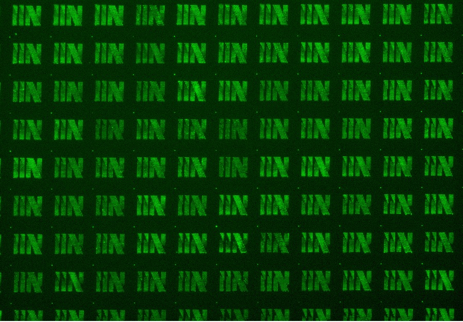
As evidence of their control over the size and location of individual nanocrystals, the researchers printed patterns of nanocrystals spelling out the letters ‘IIN’ in the actual logo font of the International Institute for Nanotechnology. Each ‘IIN’ was 100 micrometers wide; the letters were composed of nanocrystal ‘dots’ as small as 50 nanometers in size.
This method made it possible to create a single-nanocrystal solar cell, capable of efficiently capturing light and translating it into energy. As miniaturized, efficient power sources that could be integrated into a microchip, nanocrystal solar cells could reduce the bulk of wearable devices like activity trackers or virtual reality headsets. These nanocrystals could also serve as sensors that activate nano-electronic devices upon detecting the presence of light.
The research also revealed new information about the way that a nanocrystal’s size can affect the light it emits, which made it possible to create RGB (red/green/blue) pixel arrays.
Mirkin’s laboratory is now using this data to develop nanocrystal LEDs, which could significantly improve the quality of televisions, smartphones, and other optical displays. Where current LEDs use comparatively bulky microcrystals to generate color, nanocrystal-based LEDs could reach a far greater pixel density due to their nanoscale size, while achieving much higher color purity and intensity. Mirkin anticipates that these displays would last longer as well.
The research, “Halide Perovskite Nanocrystal Arrays: Multiplexed Synthesis and Size-dependent Emission,” was supported by the Air Force Office of Scientific Research, the Sherman Fairchild Foundation, and the National Science Foundation. Donghoon Shin, Teodor K. Stanev, Chiara Musumeci, Zhuang Xie, Ziyin Huang, Minliang Lai, Lin Sun, Wenjie Zhou, and Nathaniel Stern — all from Northwestern — co-authored the paper.
Note: A patent application has been submitted for this work. Mirkin has financial interests in TERA-print, LLC, which could potentially benefit from the outcomes of this research.